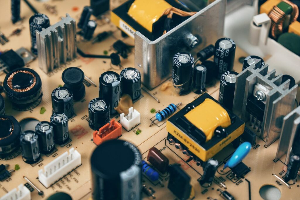
- SMT: Surface Mount Technology
- PCB: Printed Circuit Board
- BGA: Ball Grid Array
- QFN: Quad Flat No-leads
- CSP: Chip Scale Package
- LGA: Land Grid Array
- QFP: Quad Flat Package
- SOIC: Small Outline Integrated Circuit
- SOP: Small Outline Package
- TQFP: Thin Quad Flat Package
- TDR: Time-domain reflectometry, a measurement technique that uses a pulse signal to measure the electrical characteristics of a PCB or SMD.
- V-score: A process of scoring or grooving the PCB substrate to make it easier to separate the PCB after assembly.
- PCB Panel: A large PCB divided into smaller individual PCBs, which are later separated and used as individual PCBs.
- Panel Array: A group of identical SMDs placed on a PCB panel in a matrix arrangement.
- PCB trace: A thin conductor on the surface of a PCB that connects one component to another.
- Via: A small hole in a PCB that connects one layer of a PCB to another or connects the surface of the PCB to an internal layer.
- Solder mask: A thin layer of polymer that covers the surface of a PCB to protect the traces and vias from damage and to provide insulation.
- Solder paste: A mixture of tiny solder particles suspended in flux that is used to create the solder joints between SMDs and a PCB.
- SMD: Surface Mount Device
- PTH: Plated Through-Hole
- BOM: Bill of Materials
- stencil: a thin metal or polymer sheet with cutouts in the shape of the SMD pads, used to apply solder paste to the PCB before components are placed.
- Reflow: The heating process that melts the solder paste and causes it to flow and solidify, creating a mechanical and electrical connection between the SMD and the PCB.
- Pick and Place: The process of loading SMDs onto a PCB using a machine.
- AOI: Automated Optical Inspection, A machine that uses cameras and software to inspect the placement and alignment of SMDs on a PCB.
- ICT: In-Circuit Test, A test that verifies the electrical functionality of a PCB by applying test signals and measuring the response.
- FCT: Functional Circuit Test, A test that verifies the functional performance of a PCB by applying real-world signals and measuring the response.
- DFM: Design for Manufacturability, the practice of designing a PCB with consideration for the capabilities and constraints of the SMT assembly process.
- DFT: Design for Testability, the practice of designing a PCB with consideration for the ability to test the functionality of the finished product.
- ESD: Electrostatic Discharge, the release of static electricity that can cause damage to electronic components.
- RoHS: Restriction of Hazardous Substances, a European Union directive that limits the use of certain hazardous materials in electronic products.
- Lead-free: A term used to describe electronic components and materials that do not contain lead in compliance with RoHS regulations.
- SIR: Surface Insulation Resistance, a measurement of the resistance to electrical leakage on the surface of an SMD.
- CT: Capacitance Test, a measurement of the capacitance of an SMD.
- LCR: Inductance, Capacitance and Resistance Test, a measurement of the inductance, capacitance and resistance of an SMD.
- TDR: Time-domain reflectometry, a measurement technique that uses a pulse signal to measure the electrical characteristics of a PCB or SMD.
- V-score: A process of scoring or grooving the PCB substrate to make it easier to separate the PCB after assembly.
- PCB Panel: A large PCB divided into smaller individual PCBs, which are later separated and used as individual PCBs.
- Panel Array: A group of identical SMDs placed on a PCB panel in a matrix arrangement.
- PCB trace: A thin conductor on the surface of a PCB that connects one component to another.
- Via: A small hole in a PCB that connects one layer of a PCB to another or connects the surface of the PCB to an internal layer.
- Solder mask: A thin layer of polymer that covers the surface of a PCB to protect the traces and vias from damage and to provide insulation.
- Solder paste: A mixture of tiny solder particles suspended in flux that is used to create the solder joints between SMDs and a PCB.
knowledge
SMF Integration FAQ
SMF Integration FAQ Get instant answers about Smart Material Flow integration, API connectivity, and system capabilities Search Search SMF Connected Systems Smart Material Flow integrates